I have simulated a basic silicon - pixel detector to retrieve the current and charge collection on the pixel.
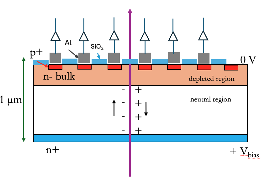
I am trying to implement a more intricate geometry for with doping concentrations on the top and bottom, including a n- bulk region and a neutral region. As such:
I have read the user guide and the MediumSilicon.hh header file, I know there is the following function:
  /// Set doping concentration [cm-3] and type ('i', 'n', 'p').
  void SetDoping(const char type, const double c);
This function sets the doping evenly throught the entire medium correct?
Is there away to restrict the doping region to create an n-bulk region and a neutral region? And possibly a lower or upper p-doping layers? Or would restricting the Area of the linear field created in ComponentUser achieve that?
Or would Garfield only be used to simulate what happens in the n-bulk region and should eliminate the neutral region from the geometry?
Dear @Khalil_Alashy
That functionality is currently not implemented a.f.a.i.k. , it would be a nice project to work on if you are interested and you have time. If you can calculate the electric field of your specific doping situation (using e.g. a TCAD simulation tool), then you can read and set the electric field as done in this example.
greets
Piet
Hi,
technically, you could create multiple MediumSilicon objects, set the doping concentration to different values, and associate the objects to different regions in your field map.
But MediumSilicon only uses the doping concentration for calculating the mobility (and only in some mobility models). At typical bulk doping concentrations, it doesn’t play a significant role.
Garfield++ does not have a built-in field solver that would enable you to calculate the electric field in a segmented, partially depleted sensor like the one in your sketch. For these applications, you would need to simulate the electric field using a TCAD device simulation program and then import the solution into Garfield++.
I will attempt for now defining multiple SolidBox (s) of MediumSilicon and lay them up in the Geometry, see if this does anything.
Although for now I am good for just simulating the behaviour around the bulk silicon without considering the top and lower layers. I’ll also look into the TCAD device system.